↧
Samsung ISOCELL Promotional Video, Part 2
↧
Article on Pixel Scaling: DTI, High-k, 0.6um Pitch, More
Semiconductor Engineering site publishes an article "Scaling CMOS Image Sensors" by Mark Lapedus. Few quotes:
Recently, vendors have ironed out the issues and the pixel scaling race has resumed. In 2018, Samsung broke the 1µm barrier with 0.9µm, followed by Sony with 0.8µm in 2019, and Samsung with 0.7µm in 2020.
For sub-µm pixel scaling, the industry requires more innovations. “As pixels shrink, thicker active (silicon) is required to maintain a suitable photodiode size,” [TechInsights analyst Ray] Fontaine said in a recent presentation. “A key technology enabler for thicker active (silicon) is DTI and associated high-k defect passivation films.”
Making an image sensor with high-k films follows a traditional flow. What’s different is that high-k films are deposited over the liner in the DTI trenches.
For high-k and other processes, vendors take two different approaches in the fab—front-DTI (F-DTI) and back-DTI (B-DTI). “F-DTI uses a poly silicon gap fill, and the poly can have voltage bias for improved surface pinning. F-DTI can also have more thermal treatment for etch damage leakage reduction,” OmniVision’s [SVP of Process Engineering Lindsay] Grant said. “B-DTI uses high-k films with a negative charge to accumulate charge and pin the Fermi level at the surface, which then suppresses dark-current leakage. The high-k film process is atomic layer deposition (ALD). B-DTI typically uses an oxide gap fill, but some metal fill and even air gap have also been tried and used in mass production.”
Will pixel scaling continue? “It’s likely that pixel scaling will continue beyond 0.7µm,” Grant said. “As pixels shrink beyond 0.7µm, many aspects need to be optimized. Key items, such as B-DTI, high-energy implant for deep diode, optical structure shrink for color and microlens, will remain the focus for development. The more basic design rules that define in-pixel transistors and interconnects need to be updated.”
Another issue is that the pixel pitch for mobile sensors is approaching the wavelength of light. “Some people may consider this a limit for minimum pixel size,” Grant said. “For example, the 0.6µm pixel pitch is used in R&D today. This is smaller than the wavelength of red light at 0.65µm (650nm). So the question may arise, ‘Why shrink to sub-wavelength? Will there be any useful benefit for the camera user? Shrinking the pixel size to sub-wavelength does not mean there is no valuable spatial resolution information at the pixel level.’”
Grant pointed out that the optical structures for a 1.0µm pixel use many sub-wavelength features. “For example, narrow metal grids for crosstalk suppression and narrow dielectric walls for quantum-efficiency are seeing improvement through light guiding. This nano-scale optical engineering is already in current pixels and has been for many years, so moving to sub-wavelength is not such a revolution,” he said. “The limitation for continued shrink may come from the user benefit rather than the technology. Today, applications continue to find end user value in shrinking the pixel size, so this is driving the trend. As long as that continues, CMOS image sensor technology development will support that direction.”
The next big thing is pixel-to-pixel interconnects. Xperi is developing a technology called “3D Hybrid BSI” for pixel-level integration. Sony and OmniVision have demonstrated the technology.
“It enables more interconnects,” said Abul Nuruzzaman, senior director of product marketing at Xperi. “It allows pixel-level interconnect between each pixel of the sensor and an associated A/D converter. This allows parallel A/D conversion for all pixels. The connection provides high-density electrical interconnection between the stacked pixel and logic layers, allowing implementation of as many A/D converters as the number of effective megapixels. Hybrid bonding can also be used to stack memory with dedicated memory to each pixel.”
↧
↧
Caeleste Proposes "True Charge Domain Binning"
Caeleste patents a true charge domain binning method by making a number of pixels “non-collecting”. The photo charge that is not collected by these pixels is then collected by drift or diffusion by the other pixels in the kernel.
While other companies might call it blooming, Caeleste implements pixel binning in that same way:
![]()
![]()
![]()
While other companies might call it blooming, Caeleste implements pixel binning in that same way:


↧
Samsung is Aiming for 600MP Sensor, IR, UV, Multispectral
Samsung publishes an article "Rivaling the Human Eye: How Samsung is Opening Up the Possibilities for Image Sensor Technology" by Yongin Park, EVP, Head of Sensor Business Team, System LSI Business. Few quotes:
"The image sensors we ourselves perceive the world through – our eyes – are said to match a resolution of around 500 megapixels (Mp). Compared to most DSLR cameras today that offer 40Mp resolution and flagship smartphones with 12Mp, we as an industry still have a long way to go to be able to match human perception capabilities.
Aiming for 600Mp for All
To date, the major applications for image sensors have been in the smartphones field, but this is expected to expand soon into other rapidly-emerging fields such as autonomous vehicles, IoT and drones. Samsung is proud to have been leading the small-pixel, high-resolution sensor trend that will continue through 2020 and beyond, and is prepared to ride the next wave of technological innovation with a comprehensive product portfolio that addresses the diverse needs of device manufacturers.
Through relentless innovation, we are determined to open up endless possibilities in pixel technologies that might even deliver image sensors that can capture more detail than the human eye."
![]()
"The image sensors we ourselves perceive the world through – our eyes – are said to match a resolution of around 500 megapixels (Mp). Compared to most DSLR cameras today that offer 40Mp resolution and flagship smartphones with 12Mp, we as an industry still have a long way to go to be able to match human perception capabilities.
Aiming for 600Mp for All
To date, the major applications for image sensors have been in the smartphones field, but this is expected to expand soon into other rapidly-emerging fields such as autonomous vehicles, IoT and drones. Samsung is proud to have been leading the small-pixel, high-resolution sensor trend that will continue through 2020 and beyond, and is prepared to ride the next wave of technological innovation with a comprehensive product portfolio that addresses the diverse needs of device manufacturers.
Through relentless innovation, we are determined to open up endless possibilities in pixel technologies that might even deliver image sensors that can capture more detail than the human eye."

↧
Heliotis White Light Interferometric 3D Sensor
Heliotis releases more info about its Series 4 while light interferometric 3D sensor:
"It’s basis is a CMOS 2D array in which each individual pixel picks up and processes the optical signal in parallel. In this SmartPixel concept each pixel has an electronic circuit for real-time image processing.
The light reflected by the sample is combined with a reference signal. This results in an interferometric signal from which the desired depth information can be derived mathematically. The system works non-invasively and non-contact in a wide range of objects and materials with a spatial resolution of microns.
The new generation of WLI sensors has been developed from scratch. We put in over 10 years of experience from Series 1, 2 and 3."
![]()
Thanks to TL for the info!
"It’s basis is a CMOS 2D array in which each individual pixel picks up and processes the optical signal in parallel. In this SmartPixel concept each pixel has an electronic circuit for real-time image processing.
The light reflected by the sample is combined with a reference signal. This results in an interferometric signal from which the desired depth information can be derived mathematically. The system works non-invasively and non-contact in a wide range of objects and materials with a spatial resolution of microns.
The new generation of WLI sensors has been developed from scratch. We put in over 10 years of experience from Series 1, 2 and 3."

Thanks to TL for the info!
↧
↧
Espros Reviews Ways to Failsafe ToF Imager
Espros April Newsletter discusses the ways to failsafe a ToF Camera:
Time-of-flight cameras are often used in safety crirical applications, e.g. in anti-collision sensors for robots. It's evident, that the sensor is working correctly or, in case of a malfunction, the control system of the of the robot detects a malfunction. A serious fault in a TOF camera is the failure of one or more pixels of the TOF imager. Whereas a «stuck--at» failure is relatively easy to detect, a floating signal which can randomly take any state is not.
A pixel in an imager can be faulty in a way that it reports any level in grayscale from fully dark to fully bright. This can also be the case in a TOF imager. Thus, in a safety critical application, the distance to an object reported by a pixel is assumed to be wrong. The pixel can report the correct distance within a given tolerance band or any other distance which is not correct. Such behavior is fatal in an anti-collision sensor based on a 3D camera. The question now is, how to detect incorrect distance reporting pixels.
There are several ways to do so:
- Comparison: Comparison of the reported distance with a known distance (comparison). This can be applied e.g. in a door sensor where the sensor looks from top of the door down to the floor.
- Offset: Adding a delay into the illumination path (or the demodulation path) to impose a virtual distance shift. By subtracting the distance shift imposed by the delay, the same or a similar distance as the one without delay should be resulting.
- Scaling: Changing the modulation frequency but not changing the distance calculation parameters accordingly. This is similar like 3., but the distance shift is not fix, it is dependent on the distance value.
- Pattern: By changing the modulation or demodulation pattern, good pixels report the same (correct) distance even in a different phase sequence.
- Fill & Spill: Inject a defined amount of charge into a pixel and check the response of the pixel.
↧
Intel Capital Imaging Portfolio: Trieye SWIR, Prophesee DVS
Avi Bakal, Trieye CEO & Co-Founder, talks about SWIR imaging in automotive applications:
Luca Verre, Prophesee CEO & Co-Founder, talks about event driven vision:
Luca Verre, Prophesee CEO & Co-Founder, talks about event driven vision:
↧
ON Semi Short Range LiDAR Demo
↧
EETimes on Event-Driven Sensor Use Cases
EETimes publishes an article "Neuromorphic Vision Sensors Eye the Future of Autonomy" by Anne-Françoise Pelé. Few quotes:
“Why do we say that an event-based vision sensor is neuromorphic? Because each pixel is a neuron, and it totally makes sense to have the artificial intelligence next to the pixel,” Pierre Cambou, principal analyst at Yole Développement (Lyon, France) told EE Times.
“It has taken awhile for us to come with a good strategy,” iniVation’s CEO Kynan Eng said in an interview. While other companies perform high-speed counting, Eng said “it is no big deal counting objects at high speed” since conventional cameras can get “a thousand frames per second, even more.” If applications don’t need to respond immediately, then “there is no point using our sensors.”
“I would [categorize] industrial vision as a relatively low risk, but low volume market,” said Eng. Hence, there has been little interest from venture funds. With an eye toward organic growth, iniVation is thinking in terms of economies of scale. Through its 2019 partnership with Samsung, iniVation shifted from manufacturing and silicon sales to selling cameras to the machine vision industry. “You can sell the $100 silicon, or you can package it in a camera and sell a $1,000 camera,” noted the Yole analyst Cambou.
“We recognized that it did not make sense for us to become a chip company,” Eng said. “We could raise a billion, and it would still not be enough to make the chip ourselves. People were asking us why our cameras were expensive and how we could make them cheap.” Partnering with Samsung, “makes that question go away.”
“A window for mobile will open in 2021 or 2022,” said Cambou. “Today, we have five cameras on the back of a Huawei phone.” Moving forward, he continued, “I don’t see anything else than an always-on neuromorphic camera. Some people talk about multispectral, but I am more thinking about always-on awareness.” An event-based camera could enable touchless interactions such as locking and unlocking phones.
Event-based cameras are power-efficient because pixel activity is insignificant; almost no energy is needed for “silent” pixels. That’s a selling point as autonomous vehicles transition from internal combustion to electric engines. For car companies, “power consumption is much more important than what I thought initially,” said Eng. “In their current planning for electric cars, if a car uses a 4kW total power budget at constant speed, half of that is for moving the car and the other half is for the computing. Every watt you can save on the compute, you can add to the range of the car or have a smaller battery.”
 |
| iniVation’s DAVIS346 DVS |
↧
↧
Samsung 108MP Nonacell Promotional Video
Samsung keeps publishing promotional videos about its image sensors. The last one presents 108MP ISOCELL Bright HM1:
↧
Prophesee Article in EETimes
EETimes publishes an article "Bringing Neuromorphic Vision to the Edge" by Jean-Luc Jaffard, Prophesee’s VP of Sensor Engineering and Operations. Few quotes:
Underlying the advantages of neuromorphic vision systems is an approach called event-based vision. Event-based vision is driving a paradigm shift away from an image capture method that has been used for more than a century: frame-based capture.
Such an approach delivers substantial advantages, including:
Many applications require high image quality not possible with event-based cameras alone. Hybrid frame/event-based approaches can utilize the best characteristics of each. With a hybridapproach, event-based vision can be used to acquire fewer frames and use asynchronous events to fill the gaps between them, which in turn reduces bandwidth and ultimately power consumption.
![]()
Underlying the advantages of neuromorphic vision systems is an approach called event-based vision. Event-based vision is driving a paradigm shift away from an image capture method that has been used for more than a century: frame-based capture.
Such an approach delivers substantial advantages, including:
- Speed — Enabled by microsecond timestamping and reduced time to action
- Data efficiency — Filtering out redundant, static data at the pixel level, before it hits the CPU
- Light sensitivity — High dynamic range and low light sensitivity
- Energy efficiency: Less power consumption for always-on, mobile and remote use cases
Many applications require high image quality not possible with event-based cameras alone. Hybrid frame/event-based approaches can utilize the best characteristics of each. With a hybridapproach, event-based vision can be used to acquire fewer frames and use asynchronous events to fill the gaps between them, which in turn reduces bandwidth and ultimately power consumption.

↧
Rise of Event Cameras
EETimes publishes Tobi Delbruck's (ETH/Zurich University) article "The Slow but Steady Rise of the Event Camera." The article refers to an excellent Github repository of event-based camera papers maintained by ETH/Zurich University.
Neuromorphic silicon retina “event camera” development languished, only gaining industrial traction when Samsung and Sony recently put their state-of-the-art image sensor process technologies on the market.
In 2017, Samsung published an ISSCC paper on a 9-um pixel, back-illuminated VGA dynamic vision sensor (DVS) using their 90-mn CIS fab. Meanwhile, Insightness announced a clever dual intensity + DVS pixel measuring a mere 7.2-um.
Both Samsung and Sony have built DVS with pixels under 5um based on stacked technologies where the back-illuminated 55-nm photosensor wafer is copper-bumped to a 28-nm readout wafer.
Similar to what occurred with CMOS image sensors, event camera startups like Insightness (recently acquired by Sony), iniVation (who carry on the iniLabs mission), Shanghai-based CelePixel and well-heeled Prophesee are established, with real products to sell. Others will surely follow.
I now think about of DVS development as mainly an industrial enterprise, but it was the heavy focus on sparse computing that has led us over the last five years to exploit activation sparsity in hardware AI accelerators. Like the spiking network in our brains, these AI accelerators only compute when needed. This approach—promoted for decades by neuromorphic engineers—is finally gaining traction in mainstream electronics.
I came up with the DVS pixel circuit. This pixel architecture is the foundation of all subsequent generations from all the major players (even when they don’t say so on their web sites).
![]()
Neuromorphic silicon retina “event camera” development languished, only gaining industrial traction when Samsung and Sony recently put their state-of-the-art image sensor process technologies on the market.
In 2017, Samsung published an ISSCC paper on a 9-um pixel, back-illuminated VGA dynamic vision sensor (DVS) using their 90-mn CIS fab. Meanwhile, Insightness announced a clever dual intensity + DVS pixel measuring a mere 7.2-um.
Both Samsung and Sony have built DVS with pixels under 5um based on stacked technologies where the back-illuminated 55-nm photosensor wafer is copper-bumped to a 28-nm readout wafer.
Similar to what occurred with CMOS image sensors, event camera startups like Insightness (recently acquired by Sony), iniVation (who carry on the iniLabs mission), Shanghai-based CelePixel and well-heeled Prophesee are established, with real products to sell. Others will surely follow.
I now think about of DVS development as mainly an industrial enterprise, but it was the heavy focus on sparse computing that has led us over the last five years to exploit activation sparsity in hardware AI accelerators. Like the spiking network in our brains, these AI accelerators only compute when needed. This approach—promoted for decades by neuromorphic engineers—is finally gaining traction in mainstream electronics.
I came up with the DVS pixel circuit. This pixel architecture is the foundation of all subsequent generations from all the major players (even when they don’t say so on their web sites).

↧
Image Sensor-Based Random Number Generator Use Cases: from Swiss Lottery to Samsung Smartphone
IDQ shows a number of use cases for its image sensor based random number generator, a Quantis QRNG Chip:
![]()
The mentioned use cases include Swiss lottery and the UK bank:
![]()
![]()
Sammobile speculates that the newest Samsung-SK Telecom Galaxy A71 5G Quantum smartphone has Quantis QRNG IDQ250C2 chip inside. IDQ states that it "is the first Quantum Random Number Generator designed and manufactured specifically for mobile handsets, IoT and edge devices." If true, the A71 Quantum has 6 image sensors: 4 inside its rear cameras, one inside a selfie camera, and one more hidden sensor inside the random number generator.
![]()
![]()

The mentioned use cases include Swiss lottery and the UK bank:


Sammobile speculates that the newest Samsung-SK Telecom Galaxy A71 5G Quantum smartphone has Quantis QRNG IDQ250C2 chip inside. IDQ states that it "is the first Quantum Random Number Generator designed and manufactured specifically for mobile handsets, IoT and edge devices." If true, the A71 Quantum has 6 image sensors: 4 inside its rear cameras, one inside a selfie camera, and one more hidden sensor inside the random number generator.


↧
↧
CIS Packaging Houses Anticipate Higher Demand: Tong Hsing, ATII
Digitimes: CIS packaging house Tong Hsing expands its wafer reconstruction capacity to support production of high-megapixel sensors for multi-lens cameras massively adopted by Chinese handset vendors for their new models.
While the handset sales in the China market may drop in 2020, the growing adoption of multi-lens camera modules and the upgrades in CIS resolution and chip sizes will contribute positively to the firm's CIS packaging business.
Tong Hsing has acquired Kingpak dedicated to BGA packaging for automotive CIS devices, seeking to form a heavyweight team to better serve global CIS makers. The world's top 5-6 CIS suppliers in Japan, South Korea, the US and Europe are expected to become clients of the expanded Tong Hsing.
Digitimes: Asia Tech Image (ATII) will expand monthly capacity at its factory in Myanmar from the curent 1.1M contact image sensors modules to 1.3M units by the end of 2020. As remote learning and working is on the rise due to the coronavirus pandemic, demand for contact image sensor modules for scanners and printers has grown significantly, according to company president Iris Wu.
![]()
While the handset sales in the China market may drop in 2020, the growing adoption of multi-lens camera modules and the upgrades in CIS resolution and chip sizes will contribute positively to the firm's CIS packaging business.
Tong Hsing has acquired Kingpak dedicated to BGA packaging for automotive CIS devices, seeking to form a heavyweight team to better serve global CIS makers. The world's top 5-6 CIS suppliers in Japan, South Korea, the US and Europe are expected to become clients of the expanded Tong Hsing.
Digitimes: Asia Tech Image (ATII) will expand monthly capacity at its factory in Myanmar from the curent 1.1M contact image sensors modules to 1.3M units by the end of 2020. As remote learning and working is on the rise due to the coronavirus pandemic, demand for contact image sensor modules for scanners and printers has grown significantly, according to company president Iris Wu.
↧
Omnivision Endoscopic Sensor Promotional Video
Omnivision publishes a promotional video about its minuscule endoscopic sensor:
Once we are at it, some time ago, Omivision sent me a season greetings with this unbelievably tiny sensor glued onto the card:
![]()
Once we are at it, some time ago, Omivision sent me a season greetings with this unbelievably tiny sensor glued onto the card:

↧
Ams dToF Sensor Video

↧
Hitachi-LG LiDAR Adapted to Check Social Distancing

↧
↧
EPFL Proposes 5T Pixel with 0.32e- Noise and Enhanced DR
IEEE Electron Device Letters gives an early access to EPFL paper "A CMOS Image Sensor Pixel Combining Deep Sub-electron Noise with Wide Dynamic Range" by Assim Boukhayma, Antonino Caizzone, and Christian Enz.
"This letter introduces a 5-transistors (5T) implementation of CMOS Image Sensors (CIS) pixels enabling the combination of deep sub-electron noise performance with wide dynamic range (DR). The 5T pixel presents a new technique to reduce the sense node capacitance without any process refinements or voltage level increase and features adjustable conversion gain (CG) to enable wide dynamic imaging. The implementation of the proposed 5T pixel in a standard 180 nm CIS process demonstrates the combination of a measured high CG of 250 μV/e- and low CG of 115 μV/e- with a saturation level of about 6500 e- offering photo-electron counting capability without compromising the DR and readout speed."
"Thanks to the high CG of 250 µV/e− and optimized PMOS SF, the read noise is as low as 0.32 e− RMS. This result is confirmed by Fig. 5 obtained by plotting the histogram of 1500 pixel outputs while the chip is exposed to very low input light. The histogram features peaks and valleys where each peak corresponds to a charge quantum."
![]()
![]()
![]()
"The reset phase consists in three steps. First, the RST switch is closed connecting IN to VRST. While VRST is set to VDD, the potential barrier between IN and SN is lowered by setting TX2 to a voltage VTX2H1 in order to dump the charge from the SN as depicted in Fig. 2(a). TX2 is set back to 0 in order to split the IN and SN and freeze the SN voltage at its maximum level.
VRST is then switched to a lower voltage VRSTL between the pin voltage of the PPD Vpin and VSN,max. After this step, the reset switch is opened again to freeze the IN voltage at a value VIN as depicted in Fig. 2(b). The last step of the reset phase consists in setting TX2 to a voltage VTX2H2 making the barrier between the IN and SN equal or slightly higher than VIN as shown in Fig. 2(c). In this way, any excess charge transferred to IN would diffuse towards the SN.
After lowering back TX2, the SN reset voltage VSN,rst is sensed. Transferring the charge integrated in the PPD to the SN takes place by pulsing both TX1 and TX2 as depicted in Fig. 2(d). TX1 is pulsed to a value VTX1H in order to set the voltage under the TG between the PPD pin voltage Vpin and the intermediate node voltage VIN while TX2 is pulsed again to transfer this charge to the SN. The signal corresponds to the difference between the SN
voltage after reset VSN,rst and the one sensed after the transfer VSN,transfer."
"This letter introduces a 5-transistors (5T) implementation of CMOS Image Sensors (CIS) pixels enabling the combination of deep sub-electron noise performance with wide dynamic range (DR). The 5T pixel presents a new technique to reduce the sense node capacitance without any process refinements or voltage level increase and features adjustable conversion gain (CG) to enable wide dynamic imaging. The implementation of the proposed 5T pixel in a standard 180 nm CIS process demonstrates the combination of a measured high CG of 250 μV/e- and low CG of 115 μV/e- with a saturation level of about 6500 e- offering photo-electron counting capability without compromising the DR and readout speed."
"Thanks to the high CG of 250 µV/e− and optimized PMOS SF, the read noise is as low as 0.32 e− RMS. This result is confirmed by Fig. 5 obtained by plotting the histogram of 1500 pixel outputs while the chip is exposed to very low input light. The histogram features peaks and valleys where each peak corresponds to a charge quantum."


"The reset phase consists in three steps. First, the RST switch is closed connecting IN to VRST. While VRST is set to VDD, the potential barrier between IN and SN is lowered by setting TX2 to a voltage VTX2H1 in order to dump the charge from the SN as depicted in Fig. 2(a). TX2 is set back to 0 in order to split the IN and SN and freeze the SN voltage at its maximum level.
VRST is then switched to a lower voltage VRSTL between the pin voltage of the PPD Vpin and VSN,max. After this step, the reset switch is opened again to freeze the IN voltage at a value VIN as depicted in Fig. 2(b). The last step of the reset phase consists in setting TX2 to a voltage VTX2H2 making the barrier between the IN and SN equal or slightly higher than VIN as shown in Fig. 2(c). In this way, any excess charge transferred to IN would diffuse towards the SN.
After lowering back TX2, the SN reset voltage VSN,rst is sensed. Transferring the charge integrated in the PPD to the SN takes place by pulsing both TX1 and TX2 as depicted in Fig. 2(d). TX1 is pulsed to a value VTX1H in order to set the voltage under the TG between the PPD pin voltage Vpin and the intermediate node voltage VIN while TX2 is pulsed again to transfer this charge to the SN. The signal corresponds to the difference between the SN
voltage after reset VSN,rst and the one sensed after the transfer VSN,transfer."
↧
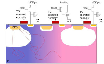
Backside Passivation
AIP paper "Backside passivation for improving the noise performance in CMOS image sensor" by Peng Sun, Sheng Hu, Wen Zou, Peng-Fei Wang, Lin Chen, Hao Zhu, Qing-Qing Sun, and David Wei Zhang from Fudan University and Wuhan Xinxin Semiconductor Manufacturing Co. analyses the passivation approaches:
"Great efforts have been made in the past few years to reduce the white pixel noise in complementary metal–oxide–semiconductor (CMOS) image sensors. As a promising approach, the surface passivation method focusing on the field-effect passivation has been studied in this work. Based on the metal–oxide–semiconductor capacitor device model, electrical measurement and analysis have been performed for characterizing the charge distribution in the system. The relationship between the flat band voltage and the white pixel performance has been set up, and the proposed passivation method that controls Si or SiO2 interface charge or traps has been proved effective in lowering the white pixel noise, which can be very attractive in improving the performance of CMOS image sensors for high-resolution and high-sensitivity applications."
![]()
![]()
![]()
"Great efforts have been made in the past few years to reduce the white pixel noise in complementary metal–oxide–semiconductor (CMOS) image sensors. As a promising approach, the surface passivation method focusing on the field-effect passivation has been studied in this work. Based on the metal–oxide–semiconductor capacitor device model, electrical measurement and analysis have been performed for characterizing the charge distribution in the system. The relationship between the flat band voltage and the white pixel performance has been set up, and the proposed passivation method that controls Si or SiO2 interface charge or traps has been proved effective in lowering the white pixel noise, which can be very attractive in improving the performance of CMOS image sensors for high-resolution and high-sensitivity applications."


↧
SPAD-based Imaging in Sunlight
University of Wisconsin-Madison ICCP 2020 presentation explains the challenges of SPAD-based ToF camera in strong ambient light:
Another presentation from the same group presents HDR imaging with SPAD camera:
Another presentation from the same group presents HDR imaging with SPAD camera:
↧