Quantcast
Channel: Image Sensors World
Viewing all 6851 articles
Browse latest View live

Pixelplus May Be Delisted from KOSDAQ

$
0
0
TheElec: South Korean PixelPlus faces a possibility of delisting from KOSDAQ stock exchange due to the four straight years of losses.

Automotive image sensors accounted for 70% to 80% of the company’s sales. 80% of its sales are in China. However, coronavirus pamndemic affected the sales and made the future forecast uncertain.

PixelPlus was founded in 2000 and initially manufactured image sensors for mobile phones. In its good times, it was listed on NASDAQ in 2005-2009. However, Samsung and Sony competition caused Pixelplus delisting from NASDAQ in 2009.

Next, PixelPlus has entered security and surveillance image sensors and was listed on KOSDAQ in 2015. However, price competition with Chinese companies was tough and Pixelplus reported yearly loss every year since 2016.

Then, PixelPlus has effectively given up on the security image sensor market and tried to enter automotive applications. These plans are frozen due to coronavirus slowdown now.


Samsung to Expand to CIS Production Capacity

$
0
0
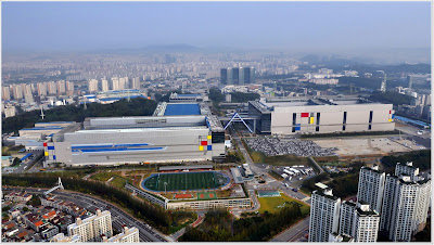
BusinessKorea: Samsung says that DRAM production line can be easily converted into an image sensor line because their processes are 80% identical. The company is preparing a detailed plan to convert part of its production lines for DRAMs in Hwaseong, Gyeonggi Province to CIS lines. The newspaper's sources say that mass production of image sensors at the converted lines can begin within this year after new equipment is installed, tested and stabilized. They claim that Samsung will spend at least one trillion won on this conversion project, although it requires less money than investment in fresh production facilities.

In 2018, the company converted part of its DRAM line 11, which is based on 300-mm (12-inch) wafers, to image sensor production line S4.

Thesis on Time to Digital Converter for SPADs

$
0
0
Universitat Politecnica Valencia, Spain, publishes MSc Thesis "Time to Digital and Charge to Digital converters for SiPM front ends" by Alessandro Morini.

"Two tasks have been carried out in this master thesis: implementation of a single front-end channel (composed by an amplifier and a gated integrator) taking into account specification have been set in advance; a survey on a Time to Digital Converter (TDC) and Analog to Digital Converter (ADC).

The first one accomplishes firstly a preamplifier for the integrated SiPM using a 0.35 um technology. The output current will feed a TDC (boosted for fast signals) and an ADC (boosted for charge integration). During the second step a gated charge integrator has been carried out, which will be used for the analog chain needed for the ADC. It has been settled an integration start threshold and a configurable integrating window.

Regarding the second task, we focused on different configurations for TDC that could work with the given requirements. Furthermore, a Sample and Hold (S/H) and a Successive Approximation ADC (SAR) have been implemented. The SAR is composed by a quite fast comparator, a programmed logic in Verilog-A, necessary to study bit by bit, and a DAC in the end.
"

Cars and Smartphones to Drive CCM Market

$
0
0
RsesearchInChina report "Global and China CMOS Camera Module (CCM) Industry Report, 2020-2026" forecasts:

"The global CCM market has been ballooning thanks to expeditious penetration of multi-camera phones and advances in automotive ADAS, being worth $22.723 billion with a year-on-year spike of 16.6% in 2019, a figure projected to sustain growth at a compound annual rate of 6.1% between 2019 and 2026.

Nowadays, single-camera, dual-camera and triple-camera mobile phones prevail globally, of which dual rear camera mobile phones share 40%. However, the upcoming triple-camera, four-camera and five-camera mobile phones will undoubtedly beat dual-camera ones, and triple-camera and four-camera phone models will become the mainstream alongside the burgeoning demand for mobile phone camera modules.

The global shipments of automotive camera modules reached 250 million units in 2019. The automotive camera module market is facilitated amid a faster rise in ADAS penetration due to the incentive policies and robust consumer demand. By 2026, the global automotive camera module shipments would expectedly hit 600 million units.

In the next few years, a growing number of camera modules will be mounted onto each mobile phone and every car.
"

Not Only Sony: Attollo Introduces SWIR Sensor with 5um Pixel Pitch

$
0
0
Attollo Engineering introduces the Phoenix, a 640 x 512 SWIR camera based on its claimed to be the industry’s smallest VGA sensor with 5 µm InGaAs pixels.

"The Attollo Phoenix SWIR camera is a VGA format (640x512), uncooled SWIR camera featuring the industry’s smallest SWIR VGA sensor - 5um pixel size. The Phoenix captures snapshot SWIR imagery using Attollo Engineering’s high‑performance InGaAs detector material and the extremely small pixel pitch enables more pixels on target with a short focal length optic. The Phoenix’s sensor is designed specifically to support broadband imaging along with day and night laser see‑spot and range-gated imaging capabilities.

The high-performance, InGaAs 640 x 512, 5 µm pixel pitch SWIR camera’s spectral response ranges from 1.0 µm to 1.65 µm with more than 99.5% operability and greater than 70% quantum efficiency. Selectable frame rates include 30 Hz, 60 Hz, 120 Hz, and 220 Hz, with windowing available. The Phoenix has a global shutter imaging mode and presets and user-defined integration time of 0.1µs (minimum), plus triggering options of sync-in (low-latency see-spot and range-gating) and sync-out. Other specifications include onboard processing with non-uniformity corrections (NUCs) and bad pixel replacement.
"

ActLight Signed Contract with "Leading Sensor Company"

$
0
0
PRNewswire: ActLight announces that it has signed a service agreement based on its Single Photon Sensitivity technology with a leading company in the sensors market.

"Even though the terms of the agreement cannot be disclosed, we are very pleased that our innovative Single Photon Sensitivity technology attracted a leading player in the sensors field," said Maxim Gureev, CTO at ActLight. "The adoption of Single Photon Avalanche Diode (SPAD) array in 3D sensing chips is growing fast. The precision of 3D sensing in applications such as smartphones, cars and smart robotics will benefit from this collaboration with our customer and our talented team of engineers is already intensively working to make it happen."

DTI and Pyramids in 0.9um Pixel Design

$
0
0
Taiwan National Cheng Kung University publishes a MDPI paper "Deep Trench Isolation and Inverted Pyramid Array Structures Used to Enhance Optical Efficiency of Photodiode in CMOS Image Sensor via Simulations" by Chang-Fu Han, Jiun-Ming Chiou, and Jen-Fin Lin. DTI and pyramids are the key elements of the modern IR-enhanced sensors from Sony, Omnivision, SmartSens, and other companies.

"The photodiode in the backside-illuminated CMOS sensor is modeled to analyze the optical performances in a range of wavelengths (300–1100 nm). The effects of changing in the deep trench isolation depth (DTI) and pitch size (d) of the inverted pyramid array (IPA) on the peak value (OEmax.) of optical efficiency (OE) and its wavelength region are identified first. Then, the growth ratio (GR) is defined for the OE change in these wavelength ranges to highlight the effectiveness of various DTI and d combinations on the OEs and evaluate the OE difference between the pixel arrays with and without the DTI + IPA structures. Increasing DTI can bring in monotonous OEmax. increases in the entire wavelength region. For a fixed DTI, the maximum OEmax. is formed as the flat plane (d = 0 nm) is chosen for the top surface of Si photodiode in the RGB pixels operating at the visible light wavelengths; whereas different nonzero value is needed to obtain the maximum OEmax. for the RGB pixels operating in the near-infrared (NIR) region. The optimum choice in d for each color pixel and DTI depth can elevate the maximum GR value in the NIR region up to 82.2%."

FLIR on SLS Sensor Advantages

$
0
0
FLIR publishes a recording of its webinar "The Advantages of SLS Cameras for R&D Applications."

"FLIR's new Type II Strained Layer Superlattice (SLS) opens up new applications and brings significant advances in thermal imaging.

Thermal imaging cameras operating in the traditional mid-wavelength IR (MWIR) tend to dominate the R&D application field due to their high sensitivity, high speed and relatively low cost compared to the cooled long-wavelength IR (LWIR) alternatives typically only accessible to military R&D professionals but the introduction of FLIRs new Type ll Strained Layer Superlattice is set to shake things up.
"


Kingpak Patents Acquired and Turned Against Other Companies

$
0
0
MaxVal reports that KT Imaging USA (KT) filed willful patent infringement complaints against Samsung Electronics, LG Electronics, Dynabook, HP, ACER and ASUSTeK in the Eastern and Western Texas District Courts. The image sensor packaging patents mentioned in the lawsuit are: US6,590,269; US6,876,544; US7,196,322; US7,511,261; US8,004,602; and US8,314,481.

KT acquired these patents from Kingpak in December of 2018. A year later, Kingpak has merged with Tong Hsing and now continues its business under Tong Hsing name.

In 2019, KT Imaging also sued Kyocera, Lightcomm Technology, and Panasonic over the same patents. The Kyocera and Panasonic lawsuits were terminated, possibly as a result of settlements, while the Lightcomm case is still pending.

MaxVal posts its summary of the patents-in-the-suits:

Assorted News: Always-On Sensors, Moon Landing LiDAR

$
0
0
Dongguk University, Seoul, Korea, publishes a MDPI paper "Design of an Always-On Image Sensor Using an Analog Lightweight Convolutional Neural Network" by Jaihyuk Choi, Sungjae Lee, Youngdoo Son, and Soo Youn Kim.

"This paper presents an always-on Complementary Metal Oxide Semiconductor (CMOS) image sensor (CIS) using an analog convolutional neural network for image classification in mobile applications. To reduce the power consumption as well as the overall processing time, we propose analog convolution circuits for computing convolution, max-pooling, and correlated double sampling operations without operational transconductance amplifiers. In addition, we used the voltage-mode MAX circuit for max pooling in the analog domain. After the analog convolution processing, the image data were reduced by 99.58% and were converted to digital with a 4-bit single-slope analog-to-digital converter. After the conversion, images were classified by the fully connected processor, which is traditionally performed in the digital domain. The measurement results show that we achieved an 89.33% image classification accuracy. The prototype CIS was fabricated in a 0.11 μm 1-poly 4-metal CIS process with a standard 4T-active pixel sensor. The image resolution was 160 × 120, and the total power consumption of the proposed CIS was 1.12 mW with a 3.3 V supply voltage and a maximum frame rate of 120."


Pixart QVGA PAJ6100U6 sensor is also aimed to always-on devices and consumes just 1.4mW at 30fps:


IEICE Electronics Express publishes Hamamatsu and Japan Aerospace Exploration Agency paper "Geiger-mode Three-dimensional Image Sensor for Eye-safe Flash LIDAR" by Takahide Mizuno, Hirokazu Ikeda, Kenji Makino, Yusei Tamura, Yoshihito Suzuki, Takashi Baba, Shunsuke Adachi, Tatsuya Hashi, Makoto Mita, Yuya Mimasu, and Takeshi Hoshino.

"Explorers attempting to land on a lunar or planetary surface must use three-dimensional image sensors to measure landing site topography for obstacle avoidance. Requirements for such sensors are similar to those mounted on vehicles and include the need for time synchronization within one frame. We introduce a 1K (32 × 32)-pixel three-dimensional image sensor using an array of InGaAs Geiger-mode avalanche photodiodes capable of photon counting in eye-safe bands and present evaluation results for sensitivity and resolution."

Eric Fossum about Past, Present, and Future of Image Sensors

200Kfps Sensor Thesis

$
0
0
University of Nevada at Las Vegas publishes a PhD Thesis "A Highly-Sensitive Global-Shutter CMOS Image Sensor with on-Chip Memory for hundreds of kilo-frames per second scientific experiments" by Konstantinos Moutafis.

"In this work, a highly-sensitive global-shutter CMOS image sensor with on-chip memory that can capture up to 16 frames at speeds higher than 200kfps is presented. The sensor fabricated and tested is a 100 x 100 pixel sensor, and was designed to be expandable to a 1000 x 1000 pixel sensor using the same building blocks and similar architecture.

The heart of the sensor is the pixel. The pixel consists of 11 transistors (11T) and 2 MOSFET capacitors. A 6T front-end is followed by a Correlated Double Sampling (CDS) circuitry that includes 2 capacitors and a reset switch. The 4T back-end circuitry consists of a source follower, in-pixel current source and 2 switches. The pixel design is unique because of the following. In a relatively small area, 15.1um x 15.1um, it performs CDS that limits the noise stored in the pixel memories to less than 0.33mV rms and allows the stored value to be read in a single readout. Moreover, it has in-pixel current source, which can be turned OFF when not in use, to remove the dependency of its output voltage to its location in the sensor. Furthermore, the in-pixel capacitors are MOSFET capacitors and do not utilize any space in the upper metal layers, therefore, they can be used exclusively for routing. And at the same time it has a fill
factor greater than 40%, which important for high sensitivity.

Each pixel is connected to a dedicated memory, which is outside the pixel array and consists of 16 MOSFET capacitors and their access switches (1T1C design). Fifty pixels share a line for their connection to their dedicated memory blocks, and, therefore, the transfer of all the stored pixel values to the on-chip memories happens within 50 clock cycles. This allows capturing consecutive frames at speeds higher than 200 kfps. The total rms noise stored in the memories is 0.4 mV.
"

Omnivision Announces 140dB HDR Automotive Sensor and DMS Wafer-Level Camera

$
0
0
BusinessWire: OmniVision announces the OX03C10 ASIL-C automotive sensor that combines a large 3.0um pixel size with HDR of 140dB and the LED flicker mitigation (LFM) for viewing applications with minimized motion artifacts. The new image sensor delivers 1920x1280p resolution at 60 fps with HDR and LFM. Additionally, the OX03C10 is said to have the lowest power consumption of any LFM image sensor with 2.5MP resolution—25% lower than the nearest competitor—along with the industry’s smallest package size, enabling the placement of cameras that continuously run at 60 fps in even the tightest spaces.

Basic image processing capabilities were also integrated into this sensor, including defect pixel correction and lens correction. The integration of OmniVision’s HALE (HDR and LFM engine) combination algorithm uniquely provides top HDR and LFM performance simultaneously.

Many stakeholders in the viewing automotive camera market are asking for higher performance, such as increased resolution, 140dB HDR and top LFM performance,” explained Pierre Cambou, Principal Analyst, Imaging from Yole Développement. “In particular, these performance increases are needed for high end CMS, also called e-Mirror, which is growing in popularity.

The OX03C10 uses our Deep Well, dual conversion gain technology to provide significantly lower motion artifacts than the few competing sensors that offer 140dB HDR,” said Kavitha Ramane, staff automotive product marketing manager at OmniVision. “Additionally, our split-pixel LFM technology with four captures provides the best performance over the entire automotive temperature range. This combination of the industry’s top HDR and LFM with a large 3.0 micron pixel enables automotive viewing system designers with the greatest image quality across all lighting conditions and in the presence of flickering LEDs from headlights, road signs and traffic signals.

OmniVision’s PureCel Plus-S stacked architecture enables pixel performance advantages over non-stacked technology. For example, 3D stacking allowed OmniVision to boost pixel and dark current performance, resulting in a 20% improvement in the signal-to-noise ratio over the prior generation of its 2.5MP viewing sensors. The OX03C10 also features 4-lane MIPI CSI-2 and 12-bit DVP interfaces.

The new OX03C10 image sensor is planned to be AEC-Q100 Grade 2 certified, and is available in both a-CSP and a-BGA packages.


BusinessWire: OmniVision announces the OVM9284 CameraCubeChip module—the world’s first automotive-grade, wafer-level camera. This 1MP module has a compact size of 6.5 x 6.5mm to provide driver monitoring system (DMS) designers with flexibility on placement within the cabin while remaining hidden from view. Additionally, it has the lowest power consumption among automotive camera modules—over 50% lower than the nearest competitor—which enables it to run continuously in the tightest of spaces and at the lowest possible temperatures for maximum image quality.

The OVM9284 is built on OmniVision’s OmniPixel 3-GS global-shutter pixel architecture, which is said to provide best-in-class QE at the 940nm. The new sensor has a 3um pixel and a 1/4" optical format, along with 1280 x 800 resolution.

The accelerated market drive for DMS is expected to generate a 43% CAGR between 2019 and 2025,” asserted Pierre Cambou. “DMS is probably the next growth story for ADAS cameras as driver distraction is becoming a major issue and has brought regulator attention.

Most existing DMS cameras use glass lenses, which are large and difficult to hide from drivers to avoid distraction, and are too expensive for most car models,” said Aaron Chiang, marketing director at OmniVision. “Our OVM9284 CameraCubeChip module is the world’s first to provide automotive designers with the small size, low power consumption and reflowable form factor of wafer-level optics.

The OVM9284’s integration of OmniVision’s image sensor, signal processor and wafer-level optics in a single compact package reduces the complexity of dealing with multiple vendors, and increases supply reliability while speeding development time. Furthermore, unlike traditional cameras, all CameraCubeChip modules are reflowable. This means they can be mounted to a printed circuit board simultaneously with other components using automated surface-mount assembly equipment, which increases quality while reducing assembly costs.


A virtual demo and Q&A for the both new products will be available at AutoSensONLINE’s virtual demo sessions, on Friday, June 12th at 10:40am (Eastern). Registration is free at: ttps://auto-sens.com/autosens-online-tickets
Plasmonic Metasurface CFA for SPAD Imager

$
0
0
OSA Optica publishes a paper "Ultralow-light-level color image reconstruction using high-efficiency plasmonic metasurface mosaic filters" by Yash D. Shah, Peter W. R. Connolly, James P. Grant, Danni Hao, Claudio Accarino, Ximing Ren, Mitchell Kenney, Valerio Annese, Kirsty G. Rew, Zoë M. Greener, Yoann Altmann, Daniele Faccio, Gerald S. Buller, and David R. S. Cumming from Glasgow University, Heriot-Watt University, UK and Boise State University, USA.

"We have fabricated a high-transmittance mosaic filter array, where each optical filter was composed of a plasmonic metasurface fabricated in a single lithographic step. This plasmonic metasurface design utilized an array of elliptical and circular nanoholes, which produced enhanced optical coupling between multiple plasmonic interactions. The resulting metasurfaces produced narrow bandpass filters for blue, green, and red light with peak transmission efficiencies of 79%, 75%, and 68%, respectively. After the three metasurface filter designs were arranged in a 64×64 format random mosaic pattern, this mosaic filter was directly integrated onto a CMOS single-photon avalanche diode detector array. Color images were then reconstructed at light levels as low as approximately 5 photons per pixel, on average, via the simultaneous acquisition of low-photon multispectral data using both three-color active laser illumination and a broadband white-light illumination source."

Princeton Instruments on Imaging Applications in Quantum Research


MIPI Completes Automotive A-PHY v1.0 Development

$
0
0
BusinessWire: The MIPI Alliance announces that development has been completed on MIPI A-PHY v1.0, a long-reach SerDes physical layer interface for automotive applications. The specification is undergoing member review, with official adoption expected within the next 90 days.

A-PHY is being developed as an asymmetric data link in a point-to-point topology, with high-speed unidirectional data, embedded bidirectional control data and optional power delivery, all over a single cable. Version 1.0 offers several core benefits:
  • Simpler system integration and lower cost: native support for devices using MIPI CSI-2 and DSI-2, ultimately eliminating the need for bridge ICs
  • Long reach: up to 15 meters
  • High performance: 5 speed gears (2, 4, 8, 12 and 16 Gbps), with a roadmap to 48 Gbps and beyond
  • High reliability: ultra-low 1E-18 packet error rate for unprecedented performance over the lifetime of a vehicle
  • High resilience: ultra-high immunity to EMC effects by virtue of a unique PHY-layer retransmission system

Rick Wietfeldt, Director, MIPI Alliance Board of Directors, presents A-PHY features:

ResearchInChina: Automotive Thermal Cameras are Too Expensive for Mass Market Cars

$
0
0
ResearchInChina publishes a report "Automotive Infrared Night Vision System Research Report, 2019-2020."

"Cadillac equipped its sedans with night vision systems early in 2000, being the world’s first to pioneer such system. Mercedes-Benz, BMW, Audi, etc. followed suit. By 2013, a dozen OEMs had installed night vision systems on their top-of-the-range models but having sold not so well to this day due to the costliness of the night vision system.

4,609 new passenger cars carrying night vision systems were sold in China in 2019, an annualized spurt of 65.6% thanks to the sales growth of Cadillac XT5, Cadillac XT6 and Hongqi H7, according to ResearchInChina.

Veoneer is a typical trailblazer that has spawned infrared night vision systems in the world, and its products have experienced four generations. Its 4th-Gen night vision system, expected in June 2020, will have improved field of view and detection distances, reduction in size, weight and cost featuring enhanced algorithms for pedestrian, animal and vehicle detection as well as supporting night time automatic emergency braking (AEB) solutions.

Boson-based thermal sensing technology from FLIR Systems has been adopted by Veoneer for its L4 autonomous vehicle production contract, planned for 2021 with a “top global automaker”. Veoneer’s system will include multiple thermal sensing cameras that provide both narrow and wide field-of-view capabilities to enhance the safety of self-driving vehicles, and that help detect and classify a broad range of common roadway objects and are especially adept at detecting people and other living things.

FLIR has been sparing no effort in the availability of infrared thermal imaging technology in automobiles. In August 2019, FLIR announced its next-generation thermal vision Automotive Development Kit (ADK) featuring the high-resolution FLIR Boson thermal camera core with a resolution of 640 × 512 for the development of self-driving cars.

Uncooled infrared imagers and detector technology remain hot in research to date In August 2019, IRay Technology released a 10-μm 1280 × 1024 uncooled infrared focal plane detector. Maxtech predicts that the unit price of uncooled thermal imaging cameras will be below $2,000 after 2021, and the sales will outnumber 3 million units.

Still, infrared cameras are too expensive for automotive use. Israel-based ADASKY, China's Dali Technology, Guide Infrared and North Guangwei Technology are working on the development and mass production of low-cost infrared thermal imagers.
"

Thesis on SWIR Thin Film Sensor Optimization

$
0
0
MSc Thesis "Optimization of Short Wavelength Infrared (SWIR) Thin Film Photodetectors" by Ahmed Abdelmagid from University of Eastern Finland and imec explains quantum dot sensors trade-offs in SWIR band:

"Quantum dots (QDs) can be a promising candidate to realize low-cost photodetectors due to its solution processability which enables the use of economical deposition techniques and the monolithic integration on the complementary metaloxide-semiconductor (CMOS) readout. Moreover, the electronic properties of QDs are dependent on both QD size and surface chemistry. Modification of quantum confinement provides control of the QD bandgap, ranging form from 0.7 to 2.1 eV which make it ideal candidate for the detection in the SWIR region. In addition, by selecting the appropriate ligand, the position of the energy levels can be tuned and therefore, n-type or p-type QDs can be achieved."

Analog CNN Integration onto Image Sensor

$
0
0
Imperial College London and Ryerson University publish Arxiv.org paper "AnalogNet: Convolutional Neural Network Inference on Analog Focal Plane Sensor Processors" by Matthew Z. Wong, Benoit Guillard, Riku Murai, Sajad Saeedi, and Paul H.J. Kelly.

"We present a high-speed, energy-efficient Convolutional Neural Network (CNN) architecture utilising the capabilities of a unique class of devices known as analog Focal Plane Sensor Processors (FPSP), in which the sensor and the processor are embedded together on the same silicon chip. Unlike traditional vision systems, where the sensor array sends collected data to a separate processor for processing, FPSPs allow data to be processed on the imaging device itself. This unique architecture enables ultra-fast image processing and high energy efficiency, at the expense of limited processing resources and approximate computations. In this work, we show how to convert standard CNNs to FPSP code, and demonstrate a method of training networks to increase their robustness to analog computation errors. Our proposed architecture, coined AnalogNet, reaches a testing accuracy of 96.9% on the MNIST handwritten digits recognition task, at a speed of 2260 FPS, for a cost of 0.7 mJ per frame."

Thesis on Printed Image Sensors

$
0
0
UCB publishes a 2017 PhD Thesis "Printed Organic Thin Film Transistors, Photodiodes, and Phototransistors for Sensing and Imaging" by Adrien Pierre.

"The signal-to-noise ratio (SNR) from a photodetector element increases with larger photoactive area, which is costly to scale up using silicon wafers and wafer-based microfabrication. On the other hand, the performance of solution-processed photodetectors and transistors is advancing considerably. It is proposed that the printability of these devices on plastic substrates can enable low-cost areal scaling for high SNR light and image sensors.

This thesis advances the performance of printed organic thin film transistor (OTFT), pho- todiode (OPD), and phototransistor (OPT) devices optimized for light and image sensing applications by developing novel printing techniques and creating new device architectures. An overview is first given on the essential figures of merit for each of these devices and the state of the art in solution-processed image sensors. A novel surface energy-patterned doc- tor blade coating technique is presented to fabricate OTFTs on flexible substrates over large areas. Using this technique, OTFTs with average mobility and on-off ratios of 0.6 cm^(2)/Vs and 10^(5) are achieved, which is competitive with amorphous silicon TFTs.

High performance OPDs are also fabricated using doctor blade coating and screen printing. These printing pro- cesses give high device yield and good controllability of photodetector performance, enabling an average specific detectivity of 3.45×10^(13) cm·Hz^(0.5)·W^(-1) that is higher than silicon photo- diodes (10^(12-13)).

Finally, organic charge-coupled devices (OCCDs) and a novel OPT device architecture based on an organic heterojunction between a donor-acceptor bulk heterojunction blend and a high mobility semiconductor that allows for a wide absorption spectrum and fast charge transport are discussed. The OPT devices not only exhibit high transistor and photodetector performance, but are also able to integrate photogenerated charge at video frame rates up to 100 frames per second with external quantum efficiencies above 100%. Applications of these devices include screen printed OTFT backplanes, large-area OPDs for pulse oximeter applications, and OPT-based image sensors.
"

Viewing all 6851 articles
Browse latest View live