Quantcast
Channel: Image Sensors World
Viewing all 6850 articles
Browse latest View live

XMC Ships Over 100 Million BSI Sensors, Mass Produces Stacked Sensors

$
0
0
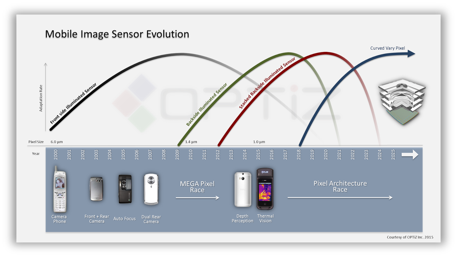
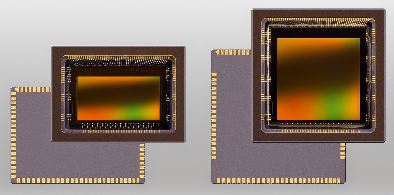
PR Newswire: XMC, a Wuhan, China-based 300mm wafer foundry, announces it has shipped over 100 million BSI CMOS image sensor units. All of the BSI CIS units are high end products ranging from 5MP to 23MP by using wafer bonding technology. In addition, the state of the art 3D wafer stacking technology developed by XMC for BSI CIS has also entered volume production now. It is said to indicate that XMC has become one of the leading BSI CIS and 3D IC manufacturing companies in the world.

The R&D of wafer-level BSI technology started in the second half of 2012. It took over one year of joint effort with an unnamed XMC's partner to reach mass production at the beginning of 2014. A year later, the more advanced 3D wafer stacking, based on the BSI technology, has also been successfully developed.

"With the offering of the advanced wafer stacking technology, XMC enables its partners to enlarge the share of high-end CIS market," Shaoning Mei, CTO at XMC said, "We will further enhance our 3D IC expertise on the basis of 3D wafer stacking technology, by which we can achieve high performance and low power through directly connecting the core parts of two chips. 3D IC is expected to be an important technology to keep us on track with Moore's Law. It is also the key strength for XMC to establish its leadership in 3D IC industry."


CMOSIS is One of the Fastest Growing Companies in Antwerp, Belgium

$
0
0
Belgian economics newspaper Trends.be names CMOSIS as one of the fastest growing companies in Antwerp, Belgium. Google translates:

"In medium businesses CMOSIS is the fastest growing. The company develops and produces image sensors for industrial, scientific and medical applications. Think of image chips for aerospace and sensors for the cameras from Leica. Also in the cameras for speed checks on Belgian roads are sensors CMOSIS. However, 99% of sales come from exports, with Germany, France, Italy, Japan, Korea, China, the US and Canada as key markets.

Sales in 2009 amounted to 1.9 million euros. In 2013 it was already 36 million, and 2014 ended with 53 million euros. "We are in a growth market - the number of cameras in our visual society will only increase," says CEO Luc De Mey that surge. "We also have as a niche player on highly sophisticated and well-patented technology, our sensors have a high image quality and a very large number of frames per second."

Since January 2014, the US investment firm TA Associates, 80% of the shares, the remaining 20% ​​is in the six founders, who are all active in the business. "As long as it goes well, we can go our own way." CMOSIS has 110 people on the payroll, including 75 in Berchem, the rest in the branches in Germany and Portugal. "The growth of our company is limited by the number of people we can find with expertise in this specialized field.
"

Zoom for Curved Sensors

$
0
0
When Sony curved sensors were presented on summer 2014, there were concerns about their compatibility with zoom lens. Palo Alto, CA-based Optiz proposes a solution. The company believes that curved sensors will be the next big wave in mobile imaging:


Optiz does not say much about the principle of its approach, other than usual marketing words:

"Optiz's proprietary Zoom solution realizes Zoom function in the mobile imaging system without the drawback of conventional solutions."

"Optiz's proprietary pixel architecture technology includes pixel pattern design, photodiode structure and advanced imaging algorithms. With inventive thinking, we have re-imagined these three crucial aspects of the pixel technology and made great advancements in zooming, luminance and color accuracy. All doing so without creating additional complexity to the imaging system while enabling zoom function and reduce module size."

"Our innovative solution offers an optical interface structure that is built into the image sensor chip, thus imaging system need fewer lenses, simplifies the overall optical design and improves image quality."

"Optiz's Zoom solution offers a set of proprietary technology to enable greater sensitivity, lower module profile, superior zooming and dynamic focusing capabilities all without moving parts."

"The innovative pixel architecture provides significant advantages such as reduced cross talk between the pixels at the periphery of the sensor, substantial improvement of Quantum efficiency."

The company has been founded by Vage Oganesian, former Tessera VP R&D, and Wang Wei, CEO of WLCSP. Few pictures from the company site might give some hints on its technology:

More Reactions on Sony CCD Decision

$
0
0
One of the biggest European machine vision camera vendors, Stemmer Imaging, posts a Q&A session with Mark Williamson, its Director of Corporate Market Development, on Sony decision to discontinue CCD products. Generally, Mark agrees that CCD era is over, although "The importance of the CCD to mankind was recognized by a Nobel prize in Physics in 2009. In the last few years there has been a big shift from CCD to CMOS in these high volume markets which has left the CCD wafer line very underutilized even with the high number of machine vision sensors sold. This makes the factory no longer financially viable."

Other quotes:

"In 2010, 22% of cameras we sold were based on CMOS sensors. This has risen to 58% in 2014 with 32% of cameras using Sony CCDs and the remainder other high end CCDs. With nearly all new camera designs using CMOS the prediction is that in a further 4 years the natural shift would make the CMOS market share approximately 80%."

"The higher end CCDs from ON Semiconductor (formerly Truesense and Kodak) and the full frame CCDs used in professional photography from Teledyne DALSA are still available for high end applications although over time CMOS will affect this market segment also."

IMV Europe too publishes an article on the Sony CCD news, mostly quoting machine vision camera vendors reports.

LCC Package Cuts CMOSIS Sensor Price in Half

$
0
0
CMOSIS is to start sampling low-cost versions of its global shutter CMV2000 (2.2MP/340fps) and CMV4000 (4.2MP/180fps) imagers in May 2015. The new versions differentiate from their CMV equivalents by their IC package, being LCC (Leadless Ceramic Carrier) instead of µPGA. The company is to offer the CMV2000/ CMV4000 imagers at about half the price of the current µPGA versions for volumes over 5000 pcs/year. Besides being lower priced, the LCC-type package offers the additional benefit of surface mount assembly, allowing more compact cameras designs and more economical camera assembly.

"We are delighted to explore new and highly attractive market segments for our proven state-of-the-art CMV product line", said Lou Hermans, COO of CMOSIS. "The LCC packaging format will open up a host of high-volume applications and further broaden our strong worldwide position and customer base for advanced camera designs."

CMOSIS sensor in the new package

Sony Confirms its Image Sensor Sales Forecast

$
0
0
Sony reports its quarterly results for the quarter ended on Jan 31, 2014. Essentially, the report confirms the company's Feb. 2015 forecast for the image sensor sales:


Sony earnings release says on Devices segment results: "Sales increased 38.6% year-on-year (a 26% increase on a constant currency basis) to 292.9 billion yen (2,421 million U.S. dollars). This significant increase was primarily due to a significant increase in sales of image sensors reflecting higher demand for mobile products, the favorable impact of foreign exchange rates, as well as a significant increase in sales of camera modules. Sales to external customers increased 47.2% year-on-year."

Dual Aperture Gets More Money from Strategic Partner

$
0
0
PRNewswire: Dual Aperture International ("DAI") announces a strategic partnership with SK Telecom ("SKT") in a development of DAI's 3D camera technology based on dual aperture 4-color (RGB-IR) sensors. SKT becomes a strategic investor and partner to DAI alongside a $1.4M investment, joining the previously closed $5.7M Series A funding round led by Korean venture capital fund Value Invest Korea.

SKT will develop applications and additional use cases for DAI's 3D image capture, virtual reality and image enhancement technologies. Prof. Chong-Min Kyung, CTO of DAI, commented that, "SKT is a global technology leader with the size and expertise to accelerate DAI's product implementation into global industries spanning mobile, medical, security and automotives. Korea already has a strong technological position in these growing industries, and the partnership between SKT and DAI will only further improve Korea's ability to provide innovative technologies and solutions to these markets."

In Korea, DAI will continue to refine its own technology while SKT will help define new applications for 3D cameras. In the US, DAI and SK Telecom Americas (SKTA) will jointly set up a consumer applications development lab under SKTA's Innopartners program in order to recruit innovators to develop new 3D, virtual reality, image related applications for various markets including Mobile, Medical, Security and Automobile applications.

DAI will also collaborate with Daejeon Creative Economy Innovation Center of the Ministry of Science, ICT and Future Planning, in actively looking for technologies and patents to foster globally competitive start-ups.

Dual Apertures technology is presented in its patent here.

Sony Stacked Sensor Features Internal Transformer

$
0
0
Chipworks reverse engineers Sony 2nd generation stacked sensor, the 13MP, 1.12um pixel IMX214, first announced about a year ago.

The main features of this stacked BSI device when compared to the respective features on the first generation stacked CIS are:
  1. refinement and modifications to the TSVs used to connect CIS signals to the ISP circuitry
  2. simplification of the manufacturing process to enable lower cost of manufacturing
  3. moving of most of the circuitry from the CIS die to the ISP die, d) changes in pixel circuitry for SME functionality
  4. changes in the organic layer stack on the light receiving side of CIS to bring microlenses closer to the pixel cathodes.

IMX214 bottom (logic) die

But the most intriguing part of the report is a small transformer somewhere on the chip:


If vias can be an indication of the transformer size, its inductance appears to be well below 100pH. Such inductors are not very useful at frequencies below 10GHz. I wonder why does Sony need it?

Update: Chipworks says that transformer part is just a generic marketing image, not related to IMX214 circuitry. The report flyer will be modified soon and the transformer image will be removed.

Another Chipworks report covers 28.2MP Samsung DSLR BSI sensor S5KVB2XX09, featuring 3.6um pixels. The highlights of this report are:
  • Samsung is the first to market with a back-illuminated APS-C format CMOS image sensor
  • An array of partially masked pixel pairs is embedded in the active pixel array to facilitate the phase-detection AF functionality
  • A new shared-pixel architecture is employed for the active pixel array

Teradyne Enhances 750 Series Testers to Support up to 128MP Image Sensors

$
0
0
Business Wire: Teradyne announced the IP750Ex-HD testers to increase the parallel test capability for both wafer and final test of image sensors using new, High Density (HD) instruments. These instruments are also compatible with over 4,000 installed J750 and IP750 test systems providing added flexibility to test system operators.

New IP750Ex-HD capabilities include:
  • HSD800 Multifunction Instrument. A third generation digital instrument providing 128 high speed digital channels, scalable to 2,048 channels per system.
  • ICMD. A new LVDS image capture instrument supporting MIPI CSI-2 D-PHY 1.5Gbps speed at 1,2,4 Data Lane CIS and Serial 1 to 16 Lane protocol support capability. This second generation instrument has 24 differential input pairs and 128M pixel capture memory .
  • IG-XL 3.60 Software.
  • Zero-footprint, Air-cooled System.
"The IP750Ex-HD uses the same HD instruments as the J750Ex-HD, which has a large installed base and TAM, providing the flexibility in manufacturing to tackle a broad range of SOC and Image Sensor devices. Adding an additional Image Capture Instrument chassis also increases the ICMD slots and allows the IP750Ex-HD to expand to higher site counts," said Jason Zee, General Manager of Teradyne's Consumer Business Unit. Teradyne has received multiple orders from multiple customers and began shipments of the IP750Ex-HD systems in the fourth quarter of 2014.

Sony Expands its Ziptronix Licensing Agreement to Multi-Million Stacked Chip Interconnects

$
0
0
Marketwired: Ziptronix announces a patent licensing agreement with Sony for application in advanced image sensors. The agreement is a continuation of the previous ZiBond agreement extended to Ziptronix's new DBI hybrid bonding patents for high volume applications.

"This license agreement with Sony is an exciting milestone for Ziptronix because it removes any doubt that our patented DBI hybrid bonding technology is both manufacturable and beneficial for high volume applications," noted Dan Donabedian, CEO and president of Ziptronix. "We believe it demonstrates that our patented hybrid bonding technology is both enabling and cost effective as compared to stacking with TSVs. Sony licensed Ziptronix's ZiBond direct bonding patents in 2011, which we also believe grew their image sensor market share from a few percent to the largest market share in the industry. We expect this new license for Ziptronix's DBI hybrid bonding patents will further contribute to Sony's growth within the industry. Any company wishing to compete in this space will need Ziptronix's DBI hybrid bonding patents."

DBI Fact Sheet lists the technology's features:

  • Interconnect pitch ≤10µm
  • Accommodates 1.5M connections/cm2
  • No adhesives, solders, pressure, underfill or wire bonding required to bond and connect layers of active devices
  • Uses standard fab tools and processes
  • Highest reliability of all 3D processes because of hermetic sealing
  • Accommodates face-to-face architectures (top die/wafer upside down)
  • Accommodates face-to-back architectures (use of through-die vias/buried contacts)

Ziptronix DBI page says:

"DBI can achieve over 100,000,000 electrical connections per square centimeter; a significant increase over the ~ 100,000 connections per square centimeter density achieved with through-die vias used in other 3D interconnect approaches."


A Youtube video shows how it works:

Xintec 12-inch WLCSP Line Ready for Mass Production in 2H 2015

$
0
0
Digitimes: Image sensor packaging house Xintec plance to have its 12-inch WLCSP production line ready 2H 2015. Xintec started to invest in its 12-inch WLP-CSP production capability in Q4 2014. TSMC holds an about 40% stake in Xintec. Orders placed by TSMC contribute about 35% to Xintec's overall revenues at present, followed by orders from OmniVision with 29%, according to Digitimes sources.

Toshiba Starts Mass Production of 13MP Sensor with Bright-Mode Video

$
0
0
Business Wire: Toshiba starts commercial production of T4K82, a 13MP, 1.12um BSI pixel sensor announced a year ago that allows smartphones and tablets to record full HD video at 240 equivalent fps, said to be the industry’s highest frame rate. Commercial shipments start today.

Cogenda Offers Image Sensor TCAD

Strategy Analytics on Vision-Based ADAS

ULIS Announces Low-Cost VGA Thermal Imager

$
0
0
ULIS announcesPico640 Gen2 low cost VGA/120fps thermal sensor for security and surveillance applications. The 17um microbolometric pixel sensor is aimed to "making thermal imaging more accessible. In addition to security and surveillance systems, ULIS’s new sensor can also be used in cameras for outdoor leisure, such as nature observation or hunting."

The new sensor's NEDT is below 50mK, a more than 15% improvement over ULIS earlier generations, without any trade-off in power consumption. It operates at less than 130mW with a 60Hz frame rate. Other thermal imaging sensors in this category are siid to consume more power, typically 200 to 350mW at an equivalent frame rate. Pico640 Gen2 is housed in ceramic packaging, a cost-saving production technique ULIS first introduced to the market ten years ago. It has shown its value and vacuum integrity in the 500,000 ULIS thermal image sensors already in the field.


Strategy Analytics: Samsung Has Largest Smartphone CIS Market Share in Units

$
0
0
Strategy Analytics publishes "Smartphone CMOS Image Sensor Market Share 2014" report. The market for CMOS image sensors in smartphones increased by 28.5% to 2.41 billion units in 2014. The smartphone image sensor market is largely dominated by Sony, Samsung and Omnivision who together accounted for almost 60% of 2014 shipments. Main camera sensors accounted for 55.4% of the total smartphone image sensor market in 2014 with front facing camera sensors accounting for the remaining 44.6% (up from 26.8% in 2010). Samsung is said to have a narrow market share lead, as measured in units.

Rambus Oversampled Pixel Patent Application

Lytro Raises $50M, Restaffs, Retargets

$
0
0
Re/code, LightField Forum: Lytro raised $50M in a round led by a new investor GSV Capital and includes participation from all of Lytro’s existing investors along with Allen & Co. and Danhua Capital. It values the company at five times its last financing round.

Lytro plans to use the new funding to make a strategic shift, taking its light-field technology into new areas, including video and virtual reality.

Lytro CEO Jason Rosenthal told Re/code “Fifty million dollars is a nice big number, but it is not unlimited. We had to make some pretty tough decisions. We are going to have to make some cuts in some areas so we can staff up in some new ones.” The company is expected to lay off 25 to 50 people out of its 130 employees, while at the same time looking to hire those with expertise in the new areas that were not previously of focus for the company.

Late last year, Lytro founder and Chairman Ren Ng announced he was leaving full-time work at the company to take a professorship at the University of California, Berkeley.

Meanwhile, Lightfield Forum reviews a recently published Lytro patent application with movable lightfield lens array to allow the camera operate in both lightfield and a regular 2D imaging mode:

ST Crolles Site Goes On Strike

Biometrics News

$
0
0
Fujitsu presents smartphone prototype with iris authentication. The active LED and camera system has been exhibited at the MWC 2015 and received the "Best Innovation Award" from AndroidPIT:


Fujitsu Youtube video in Japanese promotes the iris ID system:


In another news, the oncoming Microsoft Windows 10 features Hello component: "Windows Hello will make Windows 10 more personal by providing instant access to your devices through biometric authentication – using your face, iris or fingerprint to unlock your devices – with technology that is significantly safer than traditional passwords. We’re working closely with our hardware partners to deliver Windows Hello-capable devices that will ship with Windows 10. We are thrilled that all OEM systems incorporating the Intel RealSense F200 sensor will fully support Windows Hello, including automatic sign-in to Windows."

"For facial or iris detection, Windows Hello uses a combination of special hardware and software to accurately verify it is you – not a picture of you or someone trying to impersonate you. The cameras use infrared technology to identify your face or iris and can recognize you in a variety of lighting conditions."

The company Youtube video explains its use cases:

Viewing all 6850 articles
Browse latest View live