Quantcast
Channel: Image Sensors World
Viewing all 6857 articles
Browse latest View live

ON Semi Announces Next Generation Automotive Sensor with LED Flicker Mitigation and ASIL B Support

$
0
0
BusinessWire: ON Semiconductor announces sampling of the LED Flicker Mitigation (LFM) technology in a new 2.3MP CMOS sensor for ADAS applications. Capable of capturing 1080p HDR video, the AR0231AT also includes features that support Automotive Safety Integrity Level B (ASIL B).

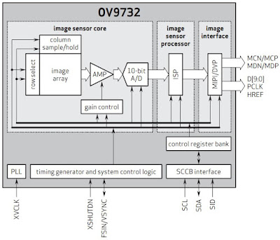
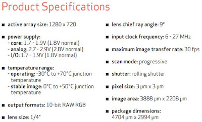
The LFM technology (patent pending) eliminates high frequency LED flicker from traffic signs and vehicle LED lighting and allows Traffic Sign Reading algorithms to operate in all light conditions. The AR0231AT has a 1/2.7-inch optical format and a 1928(H) x 1208(V) active pixel array. It uses the latest 3.0um BSI pixel with DR-Pix dual conversion gain technology. It captures images in linear, HDR or LFM modes, and offers frame-to-frame context switching between modes.

The new device offers up to 4-exposure HDR, capturing more than 120 dB dynamic range with superior noise performance. The AR0231AT is capable of multi-camera synchronization support to ease implementation in vehicle applications with multiple sensor nodes, and user programmability is achieved via a simple two-wire serial interface. It also has multiple data interfaces including MIPI, parallel and HiSPi. Other key features include selectable automatic or user controlled black level control, spread-spectrum input clock support and multiple color filter array options.

Features that support LFM and ASIL B in a 2.3 MP, 1080p BSI image sensor represent a state of the art combination ideal for high performance automotive ADAS cameras,” said Alvin Wong, senior director, Automotive Imaging and Scanning Division at ON Semiconductor.

The AR0231AT engineering samples are available now. It will be available in mass production in 2016.

Olympus 2-layer RGB-IR Stacked Sensor

$
0
0
IEDM 2015 publishes the conference preview with few pictures from Olympus paper:

Paper 30.1 – “Multi-Storied Photodiode CMOS Image Sensor for Multiband Imaging with 3D Technology” Y. Takemoto, et al, Olympus

"Multiband Imaging in One Device: There is a growing demand for integrated imaging systems that can simultaneously capture both red-green-blue (RGB) visible light and near-infrared (NIR) wavelengths that contain range-finding, or depth-of-field, information. In medicine, for example, the ability to capture all of these wavelengths simultaneously with one compact device would make it easier and less time-consuming to identify and pinpoint a wide range of targets in different parts of the body, such as pathological lesions. Until now, however, trying to detect both RGB and NIR signals on the same chip would compromise either one or the other. Researchers at Olympus will detail how they used 3D wafer-stacking technology to integrate two separate CMOS imagers into one device, each optimized for either RGB or NIR through a careful balance of active silicon thickness and pixel size. The top imager is optimized for visible detection with an array of small pixels and a thinned 3µm active silicon layer. NIR signals pass through it to reach the bottom imager, which is optimized for NIR detection with an array of larger pixels and thick active silicon. The researchers say there is no degradation in color reproduction, sensitivity or resolution."

Samsung Presentation on Mobile CIS

ON Semi Presentation on Clarity+, More

Intersil Announces ToF Processor

$
0
0
PRNewswire: Intersil introduces a ToF signal processing IC that provides a complete object detection and distance measurement when combined with an external emitter (LED or laser) and photodiode. The ISL29501 ToF device is said to offer one-of-a-kind functionality, including ultra-small size, low-power consumption and superior performance for IoT, as well as consumer mobile devices and the emerging commercial drone market.

The ISL29501 overcomes the shortcomings of traditional amplitude-based proximity sensors and other ToF solutions that perform poorly in lighting conditions above 2,000 lux, or cannot provide distance information unless the object is perpendicular to the sensor. Alternative solutions are too expensive, bulky or power hungry for use in small form factor, battery-powered applications. Based on Intersil's patented technology, the ISL29501 sensor provides a small solution footprint and precision long-range accuracy up to two meters in both dark and bright ambient light conditions. Unlike competitive solutions, the ISL29501 allows customers to select the emitter and photodiode of their choice and configure a low power ToF sensing system customized for their application.

"Prior to Intersil's time-of-flight technology breakthrough, there was no practical way to measure distance up to two meters in a small form factor," said Andrew Cowell, senior vice president of Mobile Power Products at Intersil. "The innovative ISL29501 provides customers a cost-effective, small footprint solution that also gives them the flexibility to use multiple devices to increase the field of view to a full 360 degrees for enhanced object detection capabilities."

Intersil has received a number of patents of ToF with ambient illumination rejection, such as US8274037 "Automatic calibration technique for time of flight (TOF) transceivers" by David W. Ritter, Philip Golden, Carl Warren Craddock and US8530819 "Direct current (DC) correction circuit for a time of flight (TOF) photodiode front end" by David W. Ritter, Philip Golden, Carl Warren Craddock, Kevin Brehmer, and US8530819 "Direct current (DC) correction circuit for a time of flight (TOF) photodiode front end" by David W. Ritter, Itaru Hiromi.

Key features:

  • On-chip DSP calculates ToF for accurate proximity detection and distance measurement up to two meters
  • Modulation frequency of 4.5MHz prevents interference with other consumer products such as IR TV remote controls that operate at 40kHz
  • On-chip emitter DAC with programmable current up to 255mA allows designers to choose the desired current level to optimize distance measurement and power budget
  • Operates in single shot mode for initial object detection and approximate distance measurement, while continuous mode improve distance accuracy
  • On-chip active ambient light rejection minimizes or eliminates the influence of ambient light during distance measurement
  • Programmable distance zones: allows the user to define three ToF distance zones for determining interrupt alerts
  • Interrupt controller generates interrupt alerts using distance measurements and user defined thresholds
  • Automatic gain control sets optimum analog signal levels to achieve best SNR response
  • Supply voltage range of 2.7V to 3.3V
  • I2C interface supports 1.8V and 3.3V bus

The ISL29501 ToF processing IC is available now in a low profile 4mm x 5mm, 24-lead TQFN package and is priced at $4.87 USD in 1k quantities.

Altek on Dual Camera Trend

Sony Mobile Sensor Presentation

Omnivision Presents PureCel Plus Pixel Technology


Socionext Ships H.264 Processor Consuming 1.3W at 4K, 30fps, Licenses CEVA ISP IP

$
0
0
Socionext (ex-Fujitsu) is now shipping its “M-8M” series, or MB86S27, a compact image processor which is the eighth-generation product from its Milbeaut Image Processor series. The MB86S27 features H.264 4K Codec Engine originally developed at Socionext, and comes with 360-degree distortion correction and other image processing functionalities suitable for video devices such as surveillance cameras, drones, action cameras and drive recorders. Its power consumption is as low as 1.3W, when operating with 4K at 30 fps.

In a separate PRNewswire release, CEVA announces that it has licensed its image processing IP for use in the Socionext new MB86S27 Milbeaut processor.

"The inclusion of the CEVA imaging and vision DSP in our Milbeaut series of image processors allows our customers achieve true product differentiation by implementing proprietary technologies and applications that can take advantage of its powerful vector processing engine," said Mitsugu Naito, CVP and Head of Business Group Ⅲ at Socionext. "The DSP offers outstanding performance, flexibility and power efficiency for implementing such advanced algorithms, making it the ideal choice for our imaging processing products."

"We are honored to welcome Socionext to the extensive list of leading companies adopting our imaging and vision DSPs for their image processor SoCs," said Gideon Wertheizer, CEO of CEVA. "Advanced computational photography and embedded vision capabilities are key differentiators in next-generation camera-enabled devices, and our DSP brings these features to Socionext's Milbeaut products in a low-power, cost efficient manner."

NHK Image Sensor Research

$
0
0
Sept. 2015 issue of NHK R&D Journal is almost entirely devoted to the image sensor projects:

Fabrication of Three-Dimensional Integrated Circuits for CMOS Image Sensors with Pixel-Parallel Signal Processing
Masahide GOTO, Kei HAGIWARA, Yoshinori IGUCHI and Hiroshi OHTAKE
ABSTRACT
We studied a three-dimensional (3D)-integrated image sensor that is capable of pixel-parallel signal processing, thereby meeting the demand for high-resolution and high-frame-rate imaging. Unlike the conventional 3D-stacked devices using through silicon vias (TSVs), which are not applicable to image sensor pixels of a few micrometers or less due to its hole diameter larger than the pixel size, we have recently developed a novel 3D-structuring method by using the direct bonding that could transfer signals vertically without using TSVs. Demonstrations are performed on 3D-CMOS inverters and 3D-ring oscillators with 101 stages through the lowtemperature hybrid bonding of Au contacts embedded in a SiO2 surface. The experimental results show that the developed technology is promising for high-density 3D-integrated circuits.

Color Image Sensor using Three Stacked Organic Photoconductive Films with Silicon Nitrides as Interlayer Insulators
Hokuto SEO, Toshikatsu SAKAI and Hiroshi OHTAKE
ABSTRACT
We are developing a color image sensor with three stacked organic photoconductive films (OPFs) sensitive to only one primary color component (red (R), green (G), or blue (B)); each OPF has a signal readout circuit. In this study, we fabricated a structure with three stacked OPFs sensitive to the R, G, or B component with a thickness of 5.8μm by using 2-μmthick silicon nitrides as interlayer insulators.

Development on Low-voltage Carrier Multiplication Film using Chalcopyrite Based Materials
Kenji KIKUCHI, Shigeyuki IMURA, Kazunori MIYAKAWA, Hiroshi OHTAKE and Misao KUBOTA
ABSTRACT
There is a need for highly sensitive imaging devices for high-resolution and high-frame-rate image sensors. We have been developing low-voltage carrier multiplication film using chalcopyrite based materials, CuIn1-xGax(Se1-ySy)2 (CIGS), to increase the sensitivity of image sensors. A gallium oxide (Ga2O3) thin layer, which functioned as a hole-blocking layer, was used for the CIGS layer to achieve low dark current. The electric and optical properties of Ga2O3/CIGS photodiodes were investigated. The quantum efficiency in the visible light range (400-700nm) was 95% at an applied voltage of 4V. Moreover, carrier multiplication phenomena were observed at applied voltages under 5V.

Development of CMOS Image Sensors Overlaid with Crystalline Selenium-based Heterojunction Photodiode
Shigeyuki IMURA, Kenji KIKUCHI, Kazunori MIYAKAWA, Hiroshi OHTAKE and Misao KUBOTA
ABSTRACT
We have been investigating highly sensitive imaging devices with crystalline selenium (c-Se) as a photosensitive layer for applications to nextgeneration ultra high-definition imaging systems. By using c-Se with a high absorption coefficient over the entire visible region instead of using silicon, which has been conventionally applied to a photoelectric conversion material, highly sensitive image sensors using avalanche multiplication in a photoelectric conversion film can be realized. In this paper, we describe the first observation of avalanche multiplication in a c-Se film fabricated on the glass substrate which exhibits external quantum efficiency of greater than 100%. Furthermore, we successfully created high resolution images by applying a uniform c-Se film to the CMOS circuits.

Selenium sensor external QE

Nikkei: Toshiba to Sell Image Sensor Business to Sony for about $163M

$
0
0
Nikkei reports that "Toshiba is in late-stage talks on selling its image sensor operations to Sony in a deal estimated at around 20 billion yen ($163 million)."

"Negotiations on the sale have reached an advanced stage. Toshiba is looking to divest its newest production facility in Oita, which can handle 300mm wafers. Besides production equipment, Sony would take over some employees as well as customer accounts, which include automakers and camera manufacturers.

Besides production equipment, Sony would take over some employees as well as customer accounts, which include automakers and camera manufacturers.

Toshiba would in effect withdraw from the image sensor market and concentrate its semiconductor investment on its more competitive memory business.

Toshiba's global market share in CMOS sensors came to just 1.9% last year, compared with 40.3% for Sony, according to Tokyo-based Techno Systems Research. Sony's investments in this business will help it fend off rising competition from Samsung Electronics.
"

Reuters confirms this story, based on its own sources.

Another Nikkei article talks about Toshiba restructuring and its hard choices:

"Toshiba has little choice but to carry out a sweeping reorganization of its presence in semiconductors. It has turned to Sony, which once sold a portion of its semiconductor operations in Nagasaki to Toshiba, only to buy it back later.

Some workers at its Oita semiconductor operations in southern Japan would go to Sony as part of the image sensor business sale.

Muromachi
[Masashi Muromachi, the new Toshiba President who started the re-org - ISW] once ran Toshiba's semiconductor operations in Oita."

The Japan Times quotes Yomiuri newspaper saying the deal will be officially announced next week.

Toshiba Oita Fab

Invisage Announces Release of Short Film Shot By its QuantumCinema Sensor

$
0
0
InVisage announces the release of “Prix”, a short film shot entirely with InVisage’s QuantumFilm smartphone camera sensor. The film is said to capture "a stunning level of detail despite dynamic lighting environments and shooting fast-moving subjects outdoors. This quality is made possible thanks to InVisage’s QuantumFilm, a quantum dot camera sensor technology."

Today, filmmakers of all types have access to HD-quality cameras through their smartphones,” said InVisage President and CEO Jess Lee. “However, achieving truly cinematic quality can be difficult without professional-grade cameras. Our expanded dynamic range capability is a major step forward in allowing smartphones to capture the tiniest of details across a wide range of lighting conditions. The results can be seen in ‘Prix,’ a charming short film about children who make their own technological innovations.


Prix film has been published on Youtube, while another Youtube video talks about the QuantumFilm advantages and gives a short Invisage office tour:

Ambarella Announces S3L H.265 SoC

$
0
0
BusinessWire: Ambarella introduced S3L, a low-power IP camera SoC that enables H.265, or HEVC video encoding in cloud-based home monitoring and mainstream professional IP cameras. S3L includes multi-exposure HDR, 180-degree fisheye lens correction and a high performance CPU for intelligent video analytics.

Our new S3L SoC family brings the low bit rate benefits of H.265 to cloud-based home monitoring and mainstream professional cameras,” said Chris Day, VP of marketing and business development at Ambarella.

Omnivision Announces Two 720p30 Imagers for Security

$
0
0
PRNewswire: OmniVision announced the OV9732 and OV9733, two power-efficient 720p30 CameraChip sensors based on OmniPixel3‑HS pixel for mainstream security systems and wireless battery-powered smart-home cameras.

The OV9732 is a traditional Bayer sensor. The OV9733 is equipped with RGB-IR pixels that can replace the traditional mechanical IR cut filter, thus simplifying the system designs and enabling the sensor to capture high quality infrared images and video, even from long ranges.

"Power consumption and image quality are among the most critical performance indicators for compact, battery-powered cameras found in new security systems and IoT-based smart-home and lifestyle cameras," said Chris Yiu, senior strategic marketing manager at OmniVision. "The extremely power-efficient OV9732 and OV9733 are 35 percent smaller than the previous-generation OV9712 CameraChip sensor, while capturing equally exceptional images. These benefits make the OV9732 and OV9733 extremely versatile imaging solutions, capable of supporting most mainstream security cameras and battery-operated camera platforms."

The sensors' narrow 9-degree CRA supports consumer-grade optical lens systems and reduces image artifacts for enhanced performance. When operating in low-power mode, the 1/4-inch OV9732 requires just 115mW to capture 720p30 video.

The OV9732 is currently in volume production and the OV9733 is expected to enter volume production in the Q4 2015.

Color Night Vision: Sony STARVIS vs SPI X27

$
0
0
Sony publishes a promotional video of its STARVIS BSI image sensor for security applications, said to excel in color night vision in starlight:


It's interesting to compare it with SPI Infrared Corp.'s X27 sensor videos, such as this one:


Nikkei: Toshiba to Transfer 1,100 Employees to Sony

$
0
0
Nikkei reports that Toshiba may transfer up to 1,100 employees, or about 40%, at its fab in Oita to Sony in conjunction with the image sensor business sale. The companies are discussing the employees transfer in late-stage negotiations on the deal.

Xerox PARC Develops Hyperspectral Imager

$
0
0
GlobeNewsWire: PARC, a Xerox company, develops "a hyperspectral imaging technology with the potential to be integrated into just about any existing imaging system. The technology demands a minimal cost and size overhead as it relies on a liquid crystal layer about as thick as a human hair."

"The PARC HSI technology endows any existing image sensor with spectral sensitivity without significantly increasing its cost or size. By sandwiching a liquid crystal layer between crossed polarizers and synchronizing the
drive of the liquid crystal with the camera’s image acquisition, the system performs interferometry between two polarizations of light that travel through the liquid crystal. The interferometric data are analyzed to provide the spectral information. Because the complexity of the device is shifted from hardware to software, the sophistication of full spectral processing is within reach anywhere images are normally taken.
"

PARC has prototyped its HSI technology by integrating a liquid crystal cell inside a commercial monochrome CMOS camera. The prototype offers the following performance:
  • 640 x 480 spatial resolution
  • Up to 80 degree field of view
  • Acquires 30 independent spectral bands in 0.4 seconds
  • Wavelength range 400 nm to 1100 nm
  • F/1.8 max aperture


An open-access PARC paper "Hyperspectral imaging with a liquid crystal polarization interferometer" by Alex Hegyi and Joerg Martini is published in Optics Express, Issue 22, Vol 23.

Light Co. Explains Its Technology

Sony and Toshiba Sign MOU on Assets Transfer

$
0
0
Sony and Toshiba announce that they have entered into a non-binding memorandum of understanding that confirms their intent to negotiate the transfer to Sony of certain Toshiba semiconductor fabrication facilities, equipment and related assets in Oita Prefecture, and also other related equipment and assets.

The parties intend to transfer fabrication facilities, equipment and related assets of Toshiba's 300mm wafer production line, mainly located at its Oita Operations. Following the transfer, Sony plans to operate the site as a production facility of Sony Semiconductor, primarily for manufacturing CMOS image sensors.

Negotiations between the parties are proceeding with a view to Toshiba outsourcing production of the semiconductor products Toshiba currently manufactures on its 300mm wafer production line to Sony Semiconductor following the transfer.

The parties also are planning to make arrangements to offer the employees of Toshiba and its affiliates, employed at the manufacturing facilities to be transferred, as well as those involved in areas such as CMOS image sensor engineering and design (approximately 1,100 employees in total), employment within the Sony Group, upon the completion of the transfer.

This acquisition will enable Sony to increase its CMOS sensors production capabilities, where further market growth is anticipated.

Withdrawing from the CMOS image sensors business will allow Toshiba to devote its resources to other products where it has a high technological advantage.

After due diligence on the semiconductor fabrication facilities, equipment and related assets to be transferred, Sony and Toshiba aim to execute legally binding definitive agreements by the end of calendar year 2015. Thereafter, Toshiba and Sony aim to complete the transfer within the fiscal year ending March 31, 2016, subject to regulatory approvals.

X-FAB Announces Industry’s First 4T CIS Process for High-Speed Applications Requiring Large Pixels

$
0
0
BusinessWire: X-FAB Silicon Foundries introduces XS018, said to be the first specialized 0.18µm CMOS process for fast and large image sensor pixels. Unlike the 4T pixels used in consumer products such as mobile phones and digital cameras, which have small sizes, the new XS018 technology is said to be the first to support high-speed large pixels required for medical and scientific applications such as computer tomography and x-ray scanners for 3D images. The XS018 process supports pixel sizes up to 200µm x 200µm with high-speed reading capability. The charge transfer time can be as short as 20ns with almost no image lag. The low dark current of less than 5pA/cm² gives designers a high SNR that allows high DR designs.

XS018 has a 3.3V core that results in a very low mask count, reducing cost if 1.8V devices are not necessary. Optionally, it can be extended for higher integration by using a 1.8V module.

The new 4T pixel cells with pinned photo diodes offer lower dark current and lower noise than the 3T cells commonly used today for large pixel designs. The pinned photo diode available with four different pinning voltages and a 3.3V n-channel MOS transistor with five different options for low-threshold voltages can be used as a SF, RST device or row SEL device in the pixel. This flexibility allows for higher voltage swing as the SF, and higher floating diffusion voltage as the RST device, diminishing image lag and increasing transfer speed. The XS018 also offers a 3.3V low-noise buried n-channel transistor that can reduce pixel noise.

According to Detlef Sommer, Business Line Manager CMOS Sensors at X-FAB, “Our customers in the medical and scientific sectors require large pixels and often large dies to handle the high-speed optical sensing their applications demand. We are pleased to meet this need with our new XS018 CMOS image sensor process – the first to support 4-transistor large pixel designs. In addition, our proven stitching process supports large dies – up to one die per wafer – giving our customers a clear edge for their advanced designs.

Viewing all 6857 articles
Browse latest View live